Package Dimensions
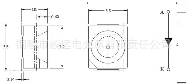 |
Notes:
1. All dimensions are in mm.
2. Tolerance is ±0.25mm unless otherwise noted.
Description
Part No. | LED Chip | Lens Color | |
Material | Emitting Color | ||
GT351LD16BMO13 | InGaN/Sapphire | White | Color Diffused |
Absolute Maximum Ratings at Ta=25℃
Parameter | Symbol | Rating | Unit |
Power Dissipation | PD | 90 | mW |
Reverse Voltage | VR | 5 | V |
D.C. Forward Current | If | 20 | mA |
Peak Current(1/10Duty Cycle,0.1ms Pulse Width.) | If(Peak) | 30 | mA |
OperatingTemperatureRange | Topr. | -40 to +75 | ℃ |
StorageTemperatureRange | Tstg. | -40 to +75 | ℃ |
Parameter | Symbol | Condition | Min. | Typ. | Max. | Unit |
Luminous Intensity | IV | If=20mA |
|
|
| mcd |
Luminous Flux | Φv | If=20mA | 30 | 32 |
| mlm |
Forward Voltage | Vf | If=20mA | 2.9 | 3.2 |
| V |
CIE Chromaticity Coordinates :X Axis | X | If=20mA |
| 0.46 |
|
|
CIE Chromaticity Coordinates :Y Axis | Y | If=20mA |
| 0.417 |
|
|
Reverse Current | Ir | Vr=5V |
|
| 10 | µA |
Correlated Colour Temperature | CCT | If=20mA |
| 6500 |
| oK |
Viewing Angle | 2θ1/2 | If=20mA |
| 120 |
| deg |
Note:1.IV is measured with an accuracy of ±5%
2.Forward voltage is measured with an accuracy of ±0.1V
COLOR RANKS (IF=20mA.Ta=25) Notes: X.Y Tolerance each Bin limit is0.01
Typical Electrical/Optical Characteristic Curves(25℃ Ambient Temperature Unless Otherwise Noted)
| |
White LED Spectrum VS. Wavelength
| |
Forward Current VS. Applied Voltage Forward Current VS. Luminous Intensity
| |
Ambient Temperature VS. Forward CurrentTemperature | Radiation Diagram |
Recommended storage environment
Temperature: 5oC ~ 30oC (41oF ~ 86oF)
Humidity: 60% RH Max.
Use within 2 days after opening of sealed vapor/ESD barrier bags.
If the moisture absorbent material (silica gel) has faded away or the LEDs have exceeded the storage time, bakingtreatment should be performed using the following conditions.
Baking treatment : 70±5℃for 24 hours.
Fold the opened bag firmly and keep in dry environment.
Soldering
| |||||||||||||||||||||||||||||||||||||||||||||
*After reflow soldering rapid cooling should be avoided.
[Temperature-profile (Surface of circuit board)]
Use the conditions shown to the under figure.
<1 : Lead Solder> <2 : Lead-free Solder>
[ Recommended soldering pad design ]
Use the following conditions shown in the figure.
+
Handling of Silicone Resin LEDs |
Handling Indications |
During processing, mechanical stress on the surface should be minimized as much as possible. Sharp objects of all types should not be used to pierce the sealing compound |
Figure 1 |
In general, LEDs should only be handled from the side. By the way, this also applies to LEDs without a silicone sealant, since the surface can also become scratched. |
Figure 2 |
When populating boards in SMT production, there are basically no restrictions regarding the form of the pick and place nozzle, except that mechanical pressure on the surface of the resin must be prevented. This is assured by choosing a pick and place nozzle which is larger than the LED’s reflector area. |

测试环境(远光的测试仪和星光的老化仪)!
| |||||||||||||||||||||||||||||||||||||||||||||
*After reflow soldering rapid cooling should be avoided.
[Temperature-profile (Surface of circuit board)]
Use the conditions shown to the under figure.
<1 : Lead Solder> <2 : Lead-free Solder>
|
[ Recommended soldering pad design ]
Use the following conditions shown in the figure.
Handling of Silicone Resin LEDs |
Handling Indications |
During processing, mechanical stress on the surface should be minimized as much as possible. Sharp objects of all types should not be used to pierce the sealing compound |
|
Figure 1 |
In general, LEDs should only be handled from the side. By the way, this also applies to LEDs without a silicone sealant, since the surface can also become scratched. |
|
Figure 2 |
When populating boards in SMT production, there are basically no restrictions regarding the form of the pick and place nozzle, except that mechanical pressure on the surface of the resin must be prevented. This is assured by choosing a pick and place nozzle which is larger than the LED’s reflector area. |
Dimensions for Tape
Dimensions for Reel
|
Notes:
1.All dimensions are in mm, tolerance is±2.0mm unless otherwise noted.
2.Specifications are subject to change without notice.
Packing
Notes:
1.All dimensions are in mm, tolerance is±2.0mm unless otherwise noted.
2.Specifications are subject to change without notice.
贴片SMD3014 3020 3528 3535 5050专业生产供应商,工厂成立十多年,现共有三家工厂,专为灯条,模组,灯具厂家研发低成本高质量的灯珠!完全不用担忧货源找不到,质量找不好,价格谈不拢的问题。你的选择您的满意。欢迎来电咨询与免费索样。供深圳工厂贴片生产线给大家参考,实物拍摄,盗图必究!