车充IC CX8506【OTP OVP OCP 短路保护 Cable补偿】欢迎来电订购:13632546861安妮
免费提供样品测试QQ:892887211 MSN:xycompass@hotmail.com
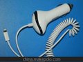
车载充电器方案
产品封装图

深圳市诚芯微科技有限公司CX918
PULSE-WIDTH-MODULATION BATTERY CHARGER
GENERAL DESCRIPTION
The CX918 is a constant current, constant voltage power supply controller, which incorporate a voltage mode, a current mode circuit, and pulse width modulation (PWM) switching regulator control circuit.
An external sense resistor will set the charge current with±8% accuracy. An internal resistor pider and precision reference set the final float voltage to 5V with±2% accuracy. With a 100 KHz switching frequency, the CX918 provides a simple solution to the EMI problem. High efficiency up to 90% will minish application component heat.
The CX918 also has over-voltage protect, over-thermal protect, and short circuit protect function. At the beginning of the charge, the over-current circuit will limit the charge current not too high. The CX918 is available in a 6-pin SOT 23-6 package.
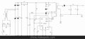
TYPICAL APPLICATION
FEATURES
z | Wide Input Supply Range: 10V to 40V |
z | High Efficiency Current Mode PWM Controller with |
| 100KHz Switching Frequency |
z | ±2% Charge Voltage Accuracy |
z | Constant Switching Frequency for Minimum Noise |
z | ±8% Charge Current Accuracy |
z | Cable compensation function |
z | Automatic Battery Recharge |
z | Automatic Shutdown When Input Supply is Removed |
z | Available in a 6-pin SOT23-6 package |
APPLICATIONS
zSMPSzChargerzPortable ComputerszHandheld Instruments
PIN DEFINITION
PIN | NAME | DESCRIPTION |
1 | VIN | Power Supply Input. |
2 | GND | The ground of IC. |
3 | VOUT | Output power supply. Connect to the external charge equipment.Note1 |
4 | SEN | Output Voltage feedback. |
5 | VCABLE | Connect an equal resistor to set the compensation voltage and improve the output power which the cable wasted. If float this pin, cable compensation function will not work. |
6 | DRV | Gate Drive Output. Driver output for the external P-Channel MOSFET. The voltage at this pin is internally clamped to 8V below VIN. |
Note1: VOUTcan be programmed to compensate the wasting voltage of cable.
ABSOLUTE MAXIMUM RATINGS
PARAMETER | SYMBOL | MIN | MAX | UNITS |
Input Supply Voltage | VIN | 10 | 40 | V |
Operating Temperature Range | TOPR | -40 | 85 | °C |
Storage Temperature Range | TSTG | -20 | 125 | °C |
Junction Temperature | θJA |
| 125 | °C |
Lead Temperature (Soldering, 10s) | TLTG | --- | 260 | °C |