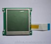
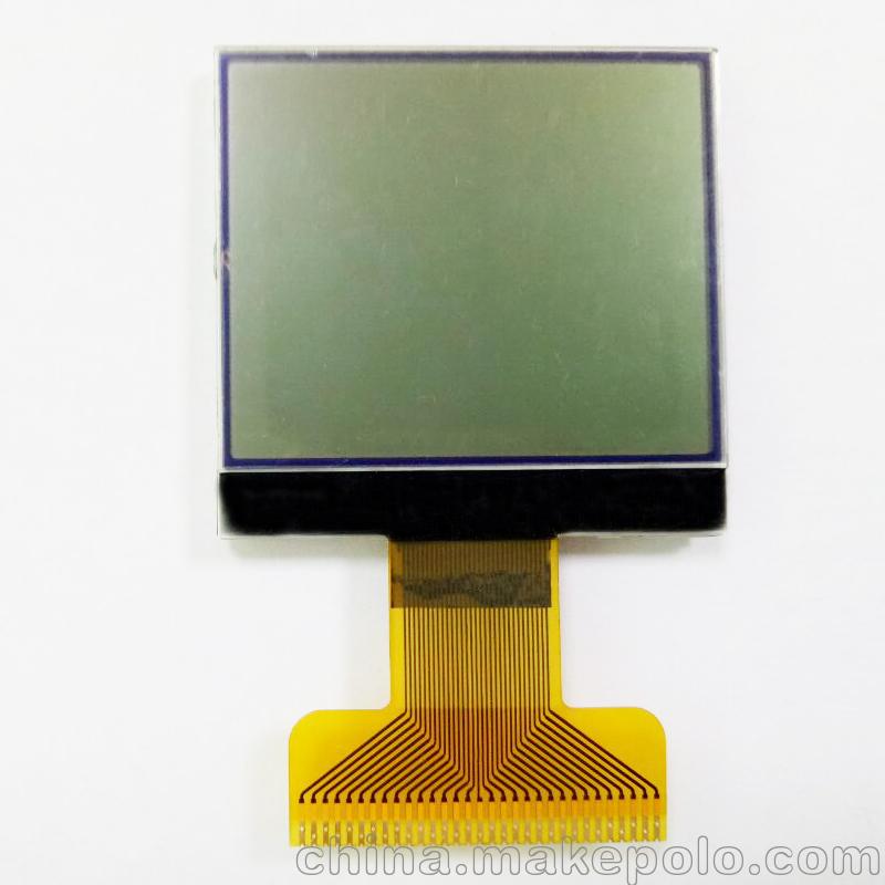
1. GENERAL DESCRIPTION
ITEM | CONTENTS |
Display Format | 128(W) × 128(H )Dots |
Color | B/W |
LCD mode | FSTN Positive |
Viewing direction | 6 O’clock |
Driving scheme | 1/128 duty, 1/10 bias, 13.0V |
Module size | 43.5(W)*42.00(H)*1.75 (T) |
Viewing area | 40.50(W)* 33.50(H) |
Dot pitch | 0.275(W)*0.23(H) |
Dot size | 0.255(W)* 0.21 (H) |
Interface | 4Line SPI/3Line SPI/Parallel 8080/Parallel 6800 |
Driver IC. | ST7571 |
Operating Temperature | -20℃~+70℃ |
Storage Temperature | -30℃~+80℃ |
Backlight | 5 white LED |
2. PIN DESCRIPTION
Pin no. | Symbol | Function |
1 | ESD | Ground |
2 | VE | It should be pull-high externally when writing EEPROM |
3 | VPP | It needs external power supply when writing EEPROM |
4 | VG | LCD driving voltage for common circuit at positive frame |
5 | VD1I/O | VD1I is the power supply pin of the internal digital circuits,VD1O is the output of the internal digital power regulator |
6 | CSEL | Select COM output sequence |
7 | VSS1 | Ground |
8 | DCPS | This pin selects the supply voltage source of the digital circuit. |
9 | OSC1 | Connect OSC1 to VDD1 |
10 | VDD1 | Power supply |
11 | XV0 | LCD driving voltage for common circuits at positive frame |
12 | V0 | LCD driving voltage for common circuits at negative frame |
13 | NC | Not connect |
14 | NC | Not connect |
15 | VMO | VMO is the output of VM |
16 | VSS | Ground |
17 | VDD | Power supply |
18 | D7(SI) | Data bus |
19 | D6 (SCL) | Data bus |
20 | D5 | Data bus |
21 | D4 | Data bus |
22 | D3 | Data bus |
23 | D2 | Data bus |
24 | D1 | Data bus |
25 | D0 | Data bus |
26 | /RD(E) | Read/Write execution pin |
27 | /WR (R/W) | Write execution control pin |
28 | RS | Register select input pin |
29 | /RESET | Reset input pin |
30 | CSB | Chip select input pin |
31 | PS1 | Select the microprocessor interface |
32 | PS0 | Select the microprocessor interface |
33 | ESD | Ground |
3.MAXIMUM ABSOUTE LIMIT (T=25°C)
Item | Symbol | Standard value | Unit |
Power supply voltage | VDD | -0.3~+3.4 | V |
Power supply voltage | LEDA | -0.3~+3.4 | V |
Operating temperature | Topr | -20~+70 | °C |
Storage temperature | Tstg | -30~+80 | °C |
Note: Voltage greater than above may damage the module
All voltages are specified relative to VSS=0V
4.ELECTRICAL CHARACTERISTICS4-1. DC Characteristics of the LCMItem | Symbol | Min | Type | Max | Unit | Test condition |
Operating voltage | VDD | 2.8 | 3.0 | 3.3 | V | - |
Supply current | IDD | - | 400 | 600 | uA | During display |
Input voltage | VIL | VSS | - | 0.2*VDD | V | - |
VIH | 0.8*VDD | - | VDD | V | ||
Output voltage | VOL | VSS | - | 0.2VDD | V | IOL=0.5mA |
VOH | 0.8VDD | - | VDD | V | IOH=-0.5mA | |
Input leakage current | ILKG | -1.0 | - | 1.0 | uA | VIN=0 or VDD |
LCD driving voltage | VLCD | 12.8 | 13.0 | 13.2 | V | V0 |
Item | Symbol | white | Unit | condition | ||
Min | Type | Max | ||||
Forward Voltage | Vf | 2.8 | 3.0 | 3.2 | V |
|
Absolute maximum forward current | If | 25/40 | 30/45 | 35/50 | mA |
|
Reverse Current | Ir | - | - | 40 | uA | Vr=5V |
Peak wave length | λp | - | - | - | nm |
|
Luminance | Lv | 200 |
|
| Cd/m2 |
|
Luminance with the LCD | Lv | TBD |
|
| Cd/m2 |
|
Lv min/ Lv max | Lv | 80 |
|
| % |
|
NO | ITEM | Symbol | Temp℃ | Rating | Unit | |||||
Min | Typ | Max | ||||||||
1 | Response | Rise time | Tr |
|
|
|
| Ms | ||
25 | N/A | 150 | 300 | |||||||
time | Fall time | Tf |
|
|
|
| ||||
25 | N/A | 150 | 300 | |||||||
2 | Operating Frequency | Ff | 25 |
| 64 |
| Hz | |||
3 | Contrast Rate | Cr | 25 | 10 | 20 | / | - | |||
4 | Viewing Direction | 6 O’CLOCK | ||||||||
5
| Viewing Angle Cr≧2
| 12Hψ=90∘ | θ1 | 25 |
| 30 |
|
Deg
| ||
6Hψ=270∘ | θ2 |
| 35 |
| ||||||
3Hψ=0∘ | θ3 |
| 30 |
| ||||||
9Hψ=180∘ | θ4 |
| 30 |
| ||||||
6 | Current Consumption | Is | 25 |
| 5.0 | 10.0 | μA | |||
7 | Capacitance | C | 25 |
| 2.0 |
| nF | |||
深圳市金彩科技有限公司 液晶显示屏(LCD),液晶显示模块(LCD Module)的生产厂家