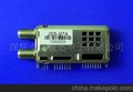
名称NAME:DVB-C 电子调谐器
DVB-C ELECTRONIC TUNER
Features
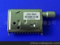
MODEL: JSS-10C
• Full frequency range from 115 to 860MHz for DVB-C
• Low IF tuner concept
• Programmable channel Filter bandwidth
• Active LT & single supply voltage
• Fully I C bus controlled
1. Brief Description
The JSS-10C are derived from –C series for digital cable reception for China
market. The half-NIM includes a full band tuner, an antenna loop through function (Active)
and channel filtering for digital signals. It provides a low IF output after channel filtering to
drive a DVB-C demodulator. Tuning, band switching and initialization are made via an I2C
bus interface. The module is built on a low-loss printed circuit board carrying all the
components in a metal housing frame with top and rear covers. The 2 aerial connectors are
mounted on one frame side all other connections are made via pins at the bottom
2. Operational Conditions
Note 1: The ripple voltage must be guaranteed in the final application.
The ripple frequency ≤ 100Hz, ≤30mVpp
3. Standard Test Conditions
Note 2: A proper function is guaranteed within the specified supply voltage and
environmental conditions but a certain deterioration of performance parameters may
ur at the limits of operational conditions.
4. Electrical Characteristics
1 nominal 3.3V, IF out Level Balanced: 1.0Vp-p Load of 1KΩ / 1pF
Note 3: IF-AGC = 1.8 Volt
Note 4: 1 at nominal, level 75dBuV for each Carrier
Antenna Active Loop through (TBD)
No Parameter Conditions
Note 5: 1 at nominal, level 75dBuV for each Carrier
5. Application Information
The module contains of one programmable part, the tuner IC TDA18250HN, which can
directly be programmed by the I2C-bus
5.1 Tuner
The source code for the TDA18250HN will be provided on request.
5.2 I2C Bus Requirements
The I2C implementation in the TDA18250HN follows the I2C bus specification, version 2.1,
January 2000 as edited by Philips Semiconductors
5.3 IC chip addresses
Write address: 0xC0, Read address: 0xC1
6.Electrostatic Discharge
6.1 Test
Each device must be capable of normal performance following its subjection to the following
tests:
MIL STD 883C HBM
Test is performed with a voltage discharge from a 100 PF capacitor over a 1500 Ω series
resistance in the discharge path. There is a direct contact between the test probe head and
the unit under test, using the test points and conditions detailed below:
Test to pins 1 through last pin : 3 essive ESD discharges of 2 KVDC between
each pin and the device frame.
Test is performed with a voltage discharge from a 150 PF capacitor over a 330 Ω series
resistance in the discharge path. There is a direct contact between the test probe head and
the unit under test, using the test points and conditions detailed below:
Test for antenna input socket 8 KVDC
Test for antenna output socket 5 KVDC
6.2 Handling
Anyone handling a device must wear a properly grounded anti - static discharge bracelet to
minimize ESD damage.
After each device is aligned and tested, it will be packed with anti - static poly-foam or material
prior to transportation and storage. This protective foam is to remain in place until the device
is assembled and soldered onto the receiver main board.
7. Reliability Test Procedure & Conditions
Note: Room temperature = 25 °C ± 2 °C
7.1 Heat Load Test
Measure the DUTs at room temperature
Load the DUTs into chamber of the following conditions:
Temperature = 60 °C
Period = 500 hrs
Cycle = 1,5 hrs on; 0,5 hrs off
Quantity = 10 pcs
Cool-down 0,5 hr at room temperature, then perform functional test on DUTs within 1hr
The test shall be continued to 1000 cycles for information only ( Optional )
7.2 Humidity Load Test
Measure the DUTs at room temperature
Load the DUTs into chamber of the following conditions:
Temperature = 40 5 °C
Period = 24 hrs
Cycle = constantly on
Quantity = 20 pcs
Cool-down 0.5 hr at room temperature, then perform functional test on DUTs within 1hr
Load the DUTs again into chamber of the following conditions:
Temperature = 40 5 °C
Humidity = 90 to 95 %
Period = 500 hrs
Cycle = 1,5 hrs on; 0,5 hrs off
Quantity = 20 pcs
Cool down 0.5 hr at room temperature, then perform functional test on DUTs within 1hr
7.3 Cold Test
Measure the DUTs at room temperature
Load the DUTs into chamber of the following conditions:
Temperature = - 20 5°C
Period = 500 hrs
Cycle = constantly on
Quantity = 10 pcs
MODEL: JSS-10C
Warm up for 2 hrs at room temperature, then perform functional test on DUTs within 1hr
7.4 Thermal Shock
Measure the DUTs at room temperature
Load the DUTs into chamber of the following conditions:
Temperature = - 25 °C for 60 min
↓ ↑
85 °C for 60 min
Period = 200 cycles
Power = power off
Quantity = 10 pcs
Cool-down 0,5 hr at room temperature then perform functional test on DUTs within 1hr
7.5 Temperature Cycle Test
Measure the DUTs at room temperature
Load the DUTs into chamber of the following conditions:
Temperature = -5 °C for 16 hrs then 60°C for 8 hrs
Period = 500 hrs
Cycle = constantly on
Quantity = 10 pcs
Cool down 0.5 hr at room temperature, then perform functional test on DUTs within 1hr
7.6 Vibration Test
Frequency: 3,5 Hz
Vertical amplitude: 15 to 25 mm
Duration: 1 hr
Quantity: 1 carton
7.7 Drop Test
Packaged apparatus: < or = 50 kg
Height: 32 … 50Kg: 0.5m
18 … 32Kg: 0.55m
10 … 18Kg: 0.65m
5 … 10Kg: 0.8m
1 corner + 3 edges + 6 faces
Quantity: 1 carton
7.8 Life Test
Measure the DUTs at room temperature
Load the DUTs into chamber of the following conditions:
Temperature = 60°C
Period = 500 hrs
Cycle = constantly on
Quantity = 20 pcs
Cool down 0.5 hr at room temperature, then perform functional test on DUTs within 1hr
8. Application diagram
Note:
1. IIC RC filtering value could be fine tune in application, for higher clock speed application we
suggest to reduce the filtering capacitor value in side tuner can having 10pF
2. Due to the miniature tuner size and the power dissipation of ~1W, therefore we mend in
chassis layout the tuner frame ground lugs the copper ground area must be sufficient to use
as heat dissipation
3. Avoid tuner place near to power supply area in application.
9. Mechanical Specification
9.1Pinning Layout on Chassis PCB
For optimum mounting of the tuner to a PCB, the PCB pinning layout (refer to relevant product
drawing) is mended
The tuner must be mounted without clearance between the tuner supporting surface and the
printed circuit board (PCB). When mounted in this way, the tuner must be soldered to the PCB.
This can be achieved by pressing the unit vertically onto the PCB during soldering
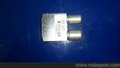
9.2 Aerial Connection
The connector, without additional support, shall withstand maximum 0.75Nm loading in 4
radial directions at the top of connector for 5 seconds, without any deformation to Cover and
no solder crack at connector.
The connector (F type only) shall withstand a torque of 2.5Nm in clockwise direction without
damage to the connector.
Tuner shall meet electrical specification after above loading conditions
9.3 Solderability
The solderability of pins and mounting tags when tested initially and after 16 hour steam
ageing in ordance with “IEC”, test TA, method 1 (solder bath 235 °C for 2 s), results in a
wetted area of 95 %. No de-wetting will ur when soldered at 260 °C for 5 s
9.4 Resistance to Soldering Heat
The product will not be damaged when tested in ordance with “IEC ”, test Tb, method 1A
(solder bath 260 °C for 10 ±1 s)
9.5 Robustness of Pins
The pins will not be damaged when tested in ordance with “IEC”
Test Ua1, tensile of 10 N in axial direction
Test Ua2, thrust of 4 N in axial direction
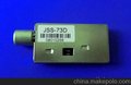
9.6 Terminal for External Connection & Outline Drawing
9.7 Pin Definitions