Product Specification
Revision | V1.1 | ||
Date | 2016-03-07 | ||
Model Name | BL-M8188NU2 | ||
Product Name | IEEE 802.11b/g/n (1T1R) Module | ||
Bilian Approve Field | |||
Engineer |
QC |
Sales | |
|
|
| |
Customer Approve Field | |||
Engineer |
QC |
Manufactory |
Purchasing |
|
|
|
|
Shenzhen Bilian Electronic Co.,Ltd
Address: No 268,Fuqian Rd.,JuTang Community ,Guanlan Town,Baoan District, Shenzhen, 518110,PRC
Homepage: www.b-link.net.cn
Table of Contents
Revision HistoryDate | Document Revision | Product Revision | Description |
2016/01/6 | 0.1 | V0.1 | Preliminary release |
2016/01/25 | 1.0 | V1.0 | Modify electrical and RF parameters;Update format |
2016/03/07 | 1.1 | V1.1 | Update format |
1. Introduction1.1 General DescriptionBL-M8188NU2 product is designed base on Realtek RTL8188EUS chipset. It operates at 2.4GHz band and supports IEEE802.11b/g/n 1T1R with wireless data rate up to 150Mbps. It supports IEEE802.11i safety protocol, along with IEEE 802.11e standard service quality. Moreover, it supports the new data encryption on 64/128 bit WEP and safety mechanism on WPA-PSK/WPA2-PSK, WPA/WPA2. It can implement the wireless network function on the laptop/desktop/MID and other wireless devices easily. Besides, this module has implemented some efficient mechanisms in its software and hardware to maximize the performance.
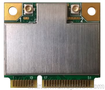
Figure 1 Top View Figure 2 Bottom View
1.2 Featuresl Frequency Range : 2.4~2.4835GHz
l Complies with USB 1.0/1.1/2.0 for WLAN
l Complies with IEEE 802.11b/g/n specification
l Wireless data rate can reach up to 150Mbps
l external antenna
l Power Supply:3.3V±0.2V
1.3 Applicationsl MID
l IP Camera
l STB
l Smart TV
l E-book
l Other devices which need to be supported by wireless network
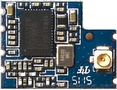
2. Functional Block Diagram
Figure 3 BL-M8188NU2 block diagram
3. Product Technical Specifications 3.1 General SpecificationsItem | Description |
Product Name | BL-M8188NU2 |
Main Chip | RTL8188EUS |
Host Interface | USB 2.0 |
IEEE Standards | IEEE 802.11b/g/n |
Frequency Range | 2.4GHz~2.4835GHz |
Modulation | 802.11b: CCK, DQPSK, DBPSK 802.11g: 64-QAM,16-QAM, QPSK, BPSK 802.11n: 64-QAM,16-QAM, QPSK, BPSK |
Working Mode | Infrastructure, Ad-Hoc |
Wireless Data Rate (Mbps) | 802.11b: 1, 2 ,5.5,11 Mbps 802.11g: 6,9,12,18,24,36,48,54 Mbps 802.11n: MCS0~7,HT20 reach up to72.2 |
Rx Sensitivity | -92dBm (Min) |
TX Power | 16±2dBm@11b, 14±2dBm@11g , 13±2dBm@11n |
Antenna Type | external antenna |
Dimension(L*W*H) | 17mm * 13mm * 0.8mm (L*W*H) ,Tolerance: ±0.15mm |
Power Supply | 3.3V±0.2V |
Power Consumption | standby mode 140mA@3.3V TX mode 245mA@3.3V |
Clock Source | 40MHz |
Working Temperature | -10°C to +50°C |
Storage Temperature | -40°C to +70°C |
ESD CAUTION: Although this module is designed to be as robust as possible, Electrostatic Discharge (ESD) can damage this module. It must be protected from ESD at all times and handled under the protection of ESD.3.2 DC Power Consumption
Vcc=3.3V,Ta = 25 °C,unit: mA | ||||
Supply current | Typ | Max | ||
Standby (RF disabled) | 82 | 86 | ||
| ||||
802.11b | 1Mbps | 11Mbps | ||
Supply current | Typ. | Max. | Typ. | Max. |
TX mode | 242 | 270 | 263 | 271 |
Rx mode | 82 | 83 | 82 | 84 |
802.11g | 6Mbps | 54Mbps | ||
Supply current | Typ. | Max. | Typ. | Max. |
TX mode | 227 | 258 | 231 | 253 |
Rx mode | 82 | 82 | 89 | 89 |
802.11n HT20 | 7.2Mbps | 72.2Mbps | ||
Supply current | Typ. | Max. | Typ. | Max. |
TX mode | 203 | 231 | 206 | 241 |
Rx mode | 82 | 82 | 82 | 83 |
802.11n HT40 | 15Mbps | 150Mbps | ||
Supply current | Typ. | Max. | Typ. | Max. |
TX mode | 203 | 225 | 209 | 240 |
Rx mode | 84 | 85 | 89 | 89 |
3.3 RF Specifications
TX Power | 802.11b:16±2dBm 802.11g:14±2dBm 802.11n:13±2dBm |
Error Vector Magnitude(EVM) | 802.11b: <-22dB@11Mbps 802.11g: <-25dB@54Mbps 802.11n-HT20: <-28dB@65Mbps 802.11n-HT40:< -28dB@150Mbps |
Receiver Minimum Input Sensitivity@PER | 1Mbps: ; 11Mbps:; 54Mbps:-72dBm@PER<10%; 65Mbps:-68dBm@PER<10%; 150Mbps:-66dBm@PER<10%; |
RF Test Report | ||||||||||
Mode | Rate(Mbps) | Power(dBm) | EVM(dB) | Sensitivity(dBm) | ||||||
CH1 | CH7 | CH13 | CH1 | CH7 | CH13 | CH1 | CH7 | CH13 | ||
11b | 1 | 15.61 | 15.63 | 16.13 | -33.92 | -35.45 | -34.19 | -96 | -96 | -96 |
5.5 | 16.11 | 15.91 | 16.72 | -24.18 | -26.06 | -27.59 | -92 | -91 | -91 | |
11 | 16.59 | 16.11 | 16.04 | -28.69 | -26.93 | -24.59 | -86 | -86 | -86 | |
11g | 9 | 14.18 | 14.40 | 14.10 | -35.20 | -33.32 | -29.68 | -90 | -90 | -89 |
36 | 14.50 | 14.13 | 14.72 | -36.20 | -33.93 | -28.03 | -81 | -80 | -80 | |
54 | 14.15 | 13.66 | 13.71 | -36.41 | -34.67 | -30.08 | -75 | -74 | -74 | |
11n HT20
| MCS0 | 13.81 | 14.31 | 14.22 | -36.44 | -31.54 | -27.86 | -90 | -90 | -90 |
MCS3 | 14.31 | 13.77 | 14.18 | -35.09 | -34.01 | -29.32 | -82 | -82 | -82 | |
MCS7 | 14.12 | 14.14 | 13.54 | -34.25 | -31.62 | -30.03 | -71 | -71 | -71 | |
Mode | Rate(Mbps) | Power(dBm) | EVM(dB) | Sensitivity(dBm) | ||||||
CH3 | CH7 | CH11 | CH3 | CH7 | CH11 | CH3 | CH7 | CH11 | ||
11n HT40 | MCS0 | 13.88 | 13.85 | 13.98 | -36.18 | -33.86 | -32.90 | -88 | -88 | -88 |
MCS3 | 14.18 | 14.03 | 14.12 | -34.92 | -34.09 | -32.25 | -79 | -79 | -79 | |
MCS7 | 13.52 | 13.41 | 14.20 | -34.15 | -34.31 | -31.69 | -68 | -68 | -68 | |
4. Pin Assignments
Figure 4 Pin Assignments (Top view)
Pin No: | Pin Name | Type | Description |
1 | VDD33 | P | VDD 3.3V |
2 | HSDM | I | USB Receive negative signal |
3 | HSDP | I | USB Receive positive signal |
4 | GND | P | Ground |
5 | GND | P | Ground |
7 | GND | P | Ground |
5. Application Information5.1 Supported Platform Operating System | CPU Framework | Driver |
WIN2000/XP/VISTA/WIN7 | X86 Platform | Enable |
LINUX2.4/2.6 | ARM, MIPSII | Enable |
WINCE5.0/6.0 | ARM ,MIPSII | Enable |
5.2 Typical Application CircuitRF reference circuit
`
NOTE:USB differential pair need to keep 90±10% ohm impedance.
6. Mechanical SpecificationsModule dimension: Typical ( L*W * H): 17mm * 13mm * 0.8mm (L*W*H) ,Tolerance: ±0.15mm
Figure 5 Top View Figure 6 Bottom View
7. Others7.1 Package Information
Figure 7 Package Information
7.2 Storage Temperature and Humidity1. Storage Condition: Moisture barrier bag must be stored under 30℃, humidity under 85% RH.
The calculated shelf life for the dry packed product shall be a 12 months from the bag seal date.
Humidity indicator cards must be blue, <30%.
2. Products require baking before mounting if humidity indicator cards reads > 30% temp < 30℃,
humidity < 70% RH, over 96 hours.
Baking condition: 125℃, 12 hours.
Baking times: 1 time.
7.3 Recommended Reflow ProfileReflow soldering shall be done according to the solder reflow profile, Typical Solder Reflow Profile is
illustrated in Figures 15. The peak temperature is 245℃.
Figure8 Typical Solder Reflow Profile