BL-R8192RD1
Product Specification
IEEE 802.11a/b/g/n (2T2R) WLAN USB Module
Version: 1.1
 Content
0. Revision History
Date | Document revision | Product revision | Change Description |
2013/05/09 | 1.0 | V1.0 | Draft initial release |
2014/03/04 | 1.1 | V1.1 | Add assembly instruction to the product specification |
1. General Description
BL-R8192RD1 product is designed base on Realtek RTL8192DU chipset .It combines CMOS MAC, Baseband PHY and RF in a single chip for IEEE 802.11a/b/g/n compatible. It supports IEEE802.11i safety protocol, along with IEEE 802.11e standard service quality. It supports the new data encryption on 64/128 bit WEP and safety mechanism on WPA-PSK/WPA2-PSK, WPA/WPA2. It can implement the wireless network function on the laptop/desktop/MID and other wireless devices easily . This module has implemented some efficient mechanisms in its software and hardware to maximize the performance.
2. Product Specification
2.1 Function Block diagram
2.2 Electrical and Performance Specification
Item | Description |
Product Name | BL-R8192RD1 |
Major Chipset | RTL8192DU-VS |
Host Interface | USB2.0 |
Standard | IEEE 802.11a, IEEE 802.11b, IEEE 802.11g,IEEE 802.11n, |
Frequency Range | 2.4GHz~2.4835GHz 5.15GHz~5.845GHz |
Modulation Type | 802.11b: CCK, DQPSK, DBPSK 802.11a/g: 64-QAM,16-QAM, QPSK, BPSK 802.11n: 64-QAM,16-QAM, QPSK, BPSK |
Working Mode | Infrastructure, Ad-Hoc |
Data Transfer Rate | 1,2,5.5,6,11,12,18,22,24,30,36,48,54,60,90,120 and maximum of 300Mbps |
Spread Spectrum | IEEE 802.11a: ISM(Industrial Scientific Medical) IEEE 802.11b: DSSS (Direct Sequence Spread Spectrum) IEEE 802.11g/n:OFDM (Orthogonal Frequency Division Multiplexing) |
Sensitivity @PER | 1M: 6M: 11M: 54:-73dBm@10%PER 135M:-68dBm@10%PER |
RF Power | < 18dBm@11b,< 14dBm@11g ,< 13dBm@11n,< 12dBm@11a |
Antenna type | Connect to the external antenna through the I-pex connector |
The transmit distance | Indoor 100M, Outdoor 300M, according the local environment |
Dimension(L*W*H) | 27.0 x 17.7 x 1.9mm (LxWxH) ;Tolerance: +-0.2mm |
Power supply | 3.3V +/-0.2V |
Power Consumption | standby mode 203mA@3.3V , TX mode 381mA@3.3V |
Clock source | 40MHz |
Working Temperature | 0ºC to +70ºC |
Storage temperature | -55°C ~ +125°C |
2.3 DC Characteristic
Symbol | Parameter | Minimum | Typical | Maximum | Units |
VD33A, VD33D | 3.3V I/O Supply Voltage | 3.135 | 3.3 | 3.465 | v |
VD12A, VD12D | 1.2V Core Supply Voltage | 1.10 | 1.2 | 1.32 | v |
VD15A, VD15D | 1.5V Supply Voltage | 1.425 | 1.5 | 1.575 | v |
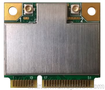
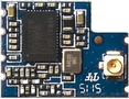
2.4 Product Photo
TOP
Bottom
2.5 Mechanical Specification
Module dimension: Typical (W x L x H): 27mmx17.7mmx1.9mm
2.6 Product Pin Definition
3. Supported platform
Operating System | CPU Framework | Driver |
WIN2000/XP/VISTA/WIN7 | X86 Platform | Enable |
LINUX2.4/2.6 | ARM, MIPSII | Enable |
WINCE5.0/6.0 | ARM ,MIPSII | Enable |
4. Peripheral Schematic Reference Design
4.1 WiFi RF Circuit reference pictures
4.2 Recommend layout pattern
RF trace need to keep 50 ohm impedance.
USB differential pair need to keep 90ohm impedance.
5. Typical Solder Reflow Profile
6. Product Assembly Instruction