供应蓝宝石片,蓝宝石衬底,蓝宝石晶片

北京嘉安恒科技有限公司
中国 北京
产品属性
图文详情
品牌推荐
品牌/厂家
北京嘉安恒科技有限公司
产品名称
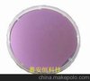
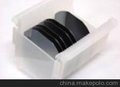
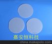
蓝宝石衬底
类型
元素半导体材料
蓝宝石晶体广泛应用于半导体(MOCVD氮化镓外延衬底基板)、钟表、医疗、通讯、激光、红外、电子、测量仪表、军工及航空航天等诸多尖端高科技领域。
| Crystal Materials | 99,996% of Al2O3,High Purity, Monocrystalline, Al2O3 | |||
| Crystal quality | Inclusions, block marks, twins, Color, micro-bubbles and dispersal centers are non-existent | |||
| Diameter | 2inch | 3inch | 4inch | 5inch ~ 7inch |
| 50.8± 0.1mm | 76.2±0.2mm | 100±0.3mm | In accordance with the provisions of standard production | |
| Thickness | 430±15µm | 550±15µm | 650±20µm | In accordance with the provisions of standard production |
| 330±15µm | 500±15µm | 550±20µm | ||
| 250±15µm | 430±15µm | 500±20µm | ||
| Orientation | C- plane (0001) to M-plane (1-100) or A-plane(1 1-2 0) 0.2±0.1° /0.3±0.1°, R-plane (1-1 0 2), A-plane (1 1-2 0 ), M-plane(1-1 0 0), Any Orientation , Any angle | |||
| Primary flat length | 16.0±0.8mm | 22.0±1.0 mm | 32.5±1.5 mm | In accordance with the provisions of standard production |
| Primary flat Orientation | A-plane (1 1-2 0 ) ± 0.2° | |||
| TTV | ≤10µm | ≤15µm | ≤20µm | ≤30µm |
| LTV | ≤10µm | ≤15µm | ≤20µm | ≤30µm |
| TIR | ≤10µm | ≤15µm | ≤20µm | ≤30µm |
| BOW | ≤10µm | ≤15µm | ≤20µm | ≤30µm |
| Warp | ≤10µm | ≤15µm | ≤20µm | ≤30µm |
| Front Surface | Epi-Polished (Ra< 0.2nm) | |||
| Back Surface | Fine ground (Ra=0.5 to 1.2 µm), Epi-Polished (Ra< 0.2nm) | |||
| Note | Can provide high-quality sapphire substrate wafer according to customers' specific requirement | |||